Designing a Microcontroller
Using RISC-V in Triple Modular Redundancy
for NASA’S Caution & Warning System
NASA – ECEN 499 Design Team
Spring 2020
Mission Statement
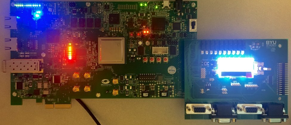
Using the PolarFire FPGA Eval kit and a custom PCB, benchmark various RISC-V core configurations in Triple Modular Redundancy (TMR) for use in NASA’s Caution and Warning System (CWS) in the Portable Life Support System (PLSS) of the newest space suit (xEMU - Exploratory Extravehicular Mobility Unit).
Microcontroller
Design
There are two main parts to this project the Libero module design and the Softconsole functions used to test and operate each of the Libero modules.
Last semester’s team left us with most of a working design for Libero. We edited the design to allow for a working Full Duplex UART and LVDS UART that transmits a differential signal but does not receive.
We did the most work with SoftConsole. We added modules to operate the LVDS and Full-Duplex UART, check status of 10 GPIO switches, we started creating functions to output text to the LCD screen and to control the operation through the large switch on the PCB, and debugged the code that wasn’t working correctly.
Hardware & Software
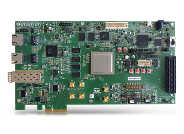
- PolarFire FPGA
- Libero
- SoftConsole
- Custom PCB - See PCB Assembly
UART
The LVDS Full-Duplex UART was set up using 3 IPs, two of them are used to create an LVDS signal and the other is used to receive and transmit UART signals. The PF_IOD_GENERIC_TX_C0_0 module turns the signal into an LVDS signal but in order to operate it we have to have clocks at different frequencies and one clock that is 90 degrees out of phase. We included the PF_CCC_C0 to generate these clock signals As for the Full-Duplex UART, all that needed to change from last semester was the settings of the UART_apb module so it is configured correctly for Full-Duplex. Using these modules, we were able to transmit a working differential UART signal that ranges between 0 volts for low and 2 volts for high.
SPI
The SPI module is an IP that was implemented when following the tutorial. It has been changed to include five extra SPI select pins to be used for a couple SPI devices on the PCB, and for some external SPI connections.
I2C
The I2C communication capabilities have been added into CPU design using a CoreI2C module. This is connected to the processor via the Advanced Peripheral Bus (APB). This module currently uses a single I2C channel set to Full Master RX/TX mode. Because this module has a separate line for input and output of the serial clock and the serial data, bi-directional buffers are used to combine them. This allows for bi-directional communication using only 2 pins.
GPIO
The GPIO pins initially came from the tutorial also, but have been modified to include 32 GPIO ports, both input and output (so they can be configured in software), and are able to send interrupts signals to the ISR.
The GPIO pins were set to both input and output and the interrupt settings were set in the settings of the Core GPIO IP module. To give them the ability to be both an input and an output, a bi-directional buffer had to be added to each GPIO port (this buffer is also used for the I2C IP). To make things look cleaner in the top Smart Design, all of this was implemented in a sub-module call GPIO_TOP.
RISC-V Implementations

We have the solution for the tutorial we followed implemented as one of our cores. Once we had a solid grasp on the CPU design process, we started from this solution and made the Solution – Copy project. That copy was fully modified to interface with the PCB and should serve as a point of reference if any problems arise. The finished copy was then saved as a separate project for more concise documentation. It was named Solution – MIV_AXI. The three other processor designs are based on this Solution – MIV_AXI. Solution – CoreRISCV replaces the processor in Solution – MIV_AXI with the CoreRISCV processor. MIV_FP and MIV_AHB are alternate processors substituted into Solution – MIV_AXI with one key difference, these two use AHB memory controllers and needed some adaptation to work with the onboard memory (they are close to completion but do require more effort yet to finish them off). All four of these last designs (the three MIV and the one CoreRISCV processors) need to be tested and then they can be benchmarked to see which one works the best.
PCB Assembly
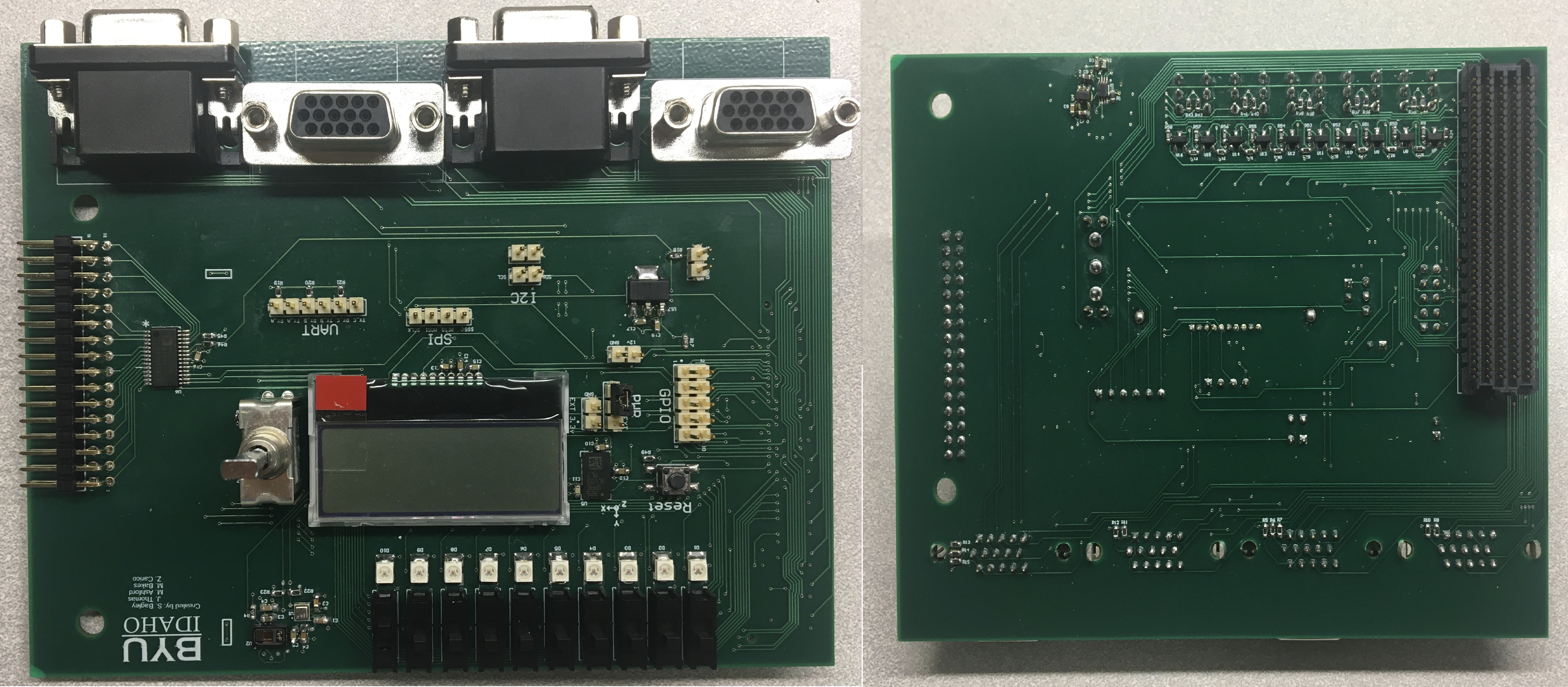
Assembling the PCB was rather straight forward. The only major hiccup was the proximity of the VGA connectors to one another. The sockets would not all be accessible at the same time for connection given their proximity to one another and the dimensions of a standard VGA cable connector. For this reason, it was decided to use VGA connectors with both 90-degree and 180-degree connections, staggering them so no two of the same were side by side.
Drivers and UI Design
Once a RISC-V core is built and loaded onto the FPGA, we can use SoftConsole, a software package to program softcores, to run our custom drivers and software on our cores. This is how we set up the interface with the PCB and how we planned on benchmarking the processors.
We used the user interface that was set up by last semesters team and added functionality to allow the FPGA to communicate over UART, check the status of GPIO pins, we started on using it to create an interface to work with the LCD screen, and debugged and fixed many of the issues used to communicate with sensors.
Future Developments
- Finish the other three processor designs
- Fix memory controller compatibility issues between AHB processors and AXI memory
- Finish the LVDS UART module in Libero
- Debug Softconsole code for LCD
- Finish implementing functions for peripheral devices in SoftConsole (Heart Rate, Accelerometer, Barometer)
- Test SPI and I2C receive functionality
Conclusions
The main goal of this semester was to get all communication, GPIO, LCD, and sensor functions created and to get one processor working with all the requirements. While we weren’t able to complete all of the requirements. We were able to get to a point when with some debugging you should be able to fix all the issues and create the functions needed to get this project working.
Even with the set backs encountered with COVID-19 we were able to nearly complete all the requirements for a single core. All that is necessary is to debug and resolve the errors with the LVDS module, add in a LVDS module for receiving data, finish the function to communicate with the LCD screen, and fully test the SPI and I2C modules. Once each of these issues are fix for the core that is alright set up it should be easy to adjust the project to work with multiple types of cores.
Acronyms
These are a few useful acronyms when working on this project:
- CWS - Caution and Warning System
- EMU - Extravehicular Mobility Unit
- FIFO - First In First Out
- FMC - FPGA Mezzanine Card
- FPGA - Field Programmable Gate Array
- HPC - High Pin Count
- IP - Intellectual Property
- LPC - Low Pin Count
- LVDS - Low Voltage Differential Signaling
- NASA - National Aeronautics and Space Administration
- PLSS - Portable Life Support System
- RISC - Reduced Instruction Set Computer
- TMR - Triple Modular Redundancy
- xEMU - Exploratory EMU
© Copyright BYUI ECEN 499, Spring 2020